


北市長候選人辯論

台北市長候選人

高雄市長候選人

邵曉鈴肇事駕駛廖俊傑

北高選舉特別報導

邵曉鈴子女公開信

多哈亞運點將錄

中華亞運台中集訓

台北市長候選人政見發表會

市長候選人謝長廷

台灣高鐵巔簸行

王建民教孩童投球

亞運女子排球捷報

林恩宇加盟樂天隊

林恩宇加盟樂天隊

圓夢巨人陳小妹

反貪腐自強晚會

旅美投手郭泓志

郭泓志手臂狀況

全台危險路段總體檢

雲林危險路段體檢

郝龍斌:郝多事要做

陳菊:港都新菊面

華視新聞請聽傾聽

降雪的兩大條件

多哈亞運圓滿落幕

王建民付費簽名
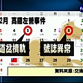
12月高鐵左營事件

2006TIME風雲人物

胡金龍陳鏞基簽名會

胡金龍為球迷簽名

陳鏞基為球迷簽名

美國塗鴉創作

美國塗鴉創作

民政局長黃呂錦如

高鐵履勘委員公開信

議會國民黨正副議長

亞運五虎將付費簽名會

2007北市跨年交管

中廣易主趙少康接手

中廣超黨派受質疑

公視氣象蕭家森

路況巔簸觀霧當心

路況巔簸觀霧當心

施工摔車北市府不理

駕駛違規項目罰鍰

台中體育場跨年晚會

台中跨年十萬人狂歡

璀璨2007跨年煙火

小巨蛋新年聲光秀

台灣本島中部地區

力霸風暴中華銀行

問題金融機構黑名單

王又曾計畫性掏空

3/1國際線申報
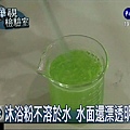
華視新聞檢驗沐浴粉

SBL打架懲處名單

高鐵捷運火警設備

子宮頸癌統計資訊
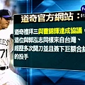
道奇與曹錦輝協議

大同公司歷史

大同公司生產線佈局

大同公司板橋廠重整

大同公司板橋廠關閉

球鞋休閒多元設計
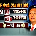
王令麟兩年還十億

2007春節訂票時間

澳網女雙冠軍賽詹莊

文化局專員陳冠甫

搶購蓋茲簽名Vista

星國遣返王又曾夫婦

王又曾夫婦抵美國

馬英九遭起訴

僑園飯店吃年夜飯

福華飯店主廚談話

台灣紅燒獅子頭

大年初四恢復收垃圾

華視晚間新聞動畫

奧斯卡金像獎特別報導

設計師作品紅毯曝光
分享:


常見的半導體材料有矽、鍺、砷化鎵等
/
晶片測試
晶片處理高度有序化的本質增加了對不同處理步驟之間度量方法的需求。晶片測試度量裝置被用於檢驗晶片仍然完好且沒有被前面的處理步驟損壞。如果If the number of dies—the 積體電路s that will eventually become chips—當一塊晶片測量失敗次數超過一個預先設定的閾值時,晶片將被廢棄而非繼續後續的處理製程。
/
晶片測試
晶片處理高度有序化的本質增加了對不同處理步驟之間度量方法的需求。晶片測試度量裝置被用於檢驗晶片仍然完好且沒有被前面的處理步驟損壞。如果If the number of dies—the 積體電路s that will eventually become chips—當一塊晶片測量失敗次數超過一個預先設定的閾值時,晶片將被廢棄而非繼續後續的處理製程。
/
步驟列表
晶片處理
濕洗
平版照相術
光刻Litho
離子移植IMP
蝕刻(干法蝕刻、濕法蝕刻、電漿蝕刻)
熱處理
快速熱退火Annel
熔爐退火
熱氧化
化學氣相沉積 (CVD)
物理氣相沉積 (PVD)
分子束磊晶 (MBE)
電化學沉積 (ECD),見電鍍
化學機械平坦化 (CMP)
IC Assembly and Testing 封裝測試
Wafer Testing 晶片測試
Visual Inspection外觀檢測
Wafer Probing電性測試
FrontEnd 封裝前段
Wafer BackGrinding 晶背研磨
Wafer Mount晶圓附膜
Wafer Sawing晶圓切割
Die attachment上片覆晶
Wire bonding焊線
BackEnd 封裝後段
Molding模壓
Post Mold Cure後固化
De-Junk 去節
Plating 電鍍
Marking 列印
Trimform 成形
Lead Scan 檢腳
Final Test 終測
Electrical Test電性測試
Visual Inspection光學測試
Baking 烘烤
/
有害材料標誌
許多有毒材料在製造過程中被使用。這些包括:
有毒元素摻雜物比如砷、硼、銻和磷
有毒化合物比如砷化三氫、磷化氫和矽烷
易反應液體、例如過氧化氫、發煙硝酸、硫酸以及氫氟酸
工人直接暴露在這些有毒物質下是致命的。通常IC製造業高度自動化能幫助降低暴露於這一類物品的風險。
/
Device yield
Device yield or die yield is the number of working chips or dies on a wafer, given in percentage since the number of chips on a wafer (Die per wafer, DPW) can vary depending on the chips' size and the wafer's diameter. Yield degradation is a reduction in yield, which historically was mainly caused by dust particles, however since the 1990s, yield degradation is mainly caused by process variation, the process itself and by the tools used in chip manufacturing, although dust still remains a problem in many older fabs. Dust particles have an increasing effect on yield as feature sizes are shrunk with newer processes. Automation and the use of mini environments inside of production equipment, FOUPs and SMIFs have enabled a reduction in defects caused by dust particles. Device yield must be kept high to reduce the selling price of the working chips since working chips have to pay for those chips that failed, and to reduce the cost of wafer processing. Yield can also be affected by the design and operation of the fab.
Tight control over contaminants and the production process are necessary to increase yield. Contaminants may be chemical contaminants or be dust particles. "Killer defects" are those caused by dust particles that cause complete failure of the device (such as a transistor). There are also harmless defects. A particle needs to be 1/5 the size of a feature to cause a killer defect. So if a feature is 100 nm across, a particle only needs to be 20 nm across to cause a killer defect. Electrostatic electricity can also affect yield adversely. Chemical contaminants or impurities include heavy metals such as Iron, Copper, Nickel, Zinc, Chromium, Gold, Mercury and Silver, alkali metals such as Sodium, Potassium and Lithium, and elements such as Aluminum, Magnesium, Calcium, Chlorine, Sulfur, Carbon, and Fluorine. It is important for those elements to not remain in contact with the silicon, as they could reduce yield. Chemical mixtures may be used to remove those elements from the silicon; different mixtures are effective against different elements.
Several models are used to estimate yield. Those are Murphy's model, Poisson's model, the binomial model, Moore's model and Seeds' model. There is no universal model; a model has to be chosen based on actual yield distribution (the location of defective chips) For example, Murphy's model assumes that yield loss occurs more at the edges of the wafer (non-working chips are concentrated on the edges of the wafer), Poisson's model assumes that defective dies are spread relatively evenly across the wafer, and Seeds's model assumes that defective dies are clustered together.[25]
Smaller dies cost less to produce (since more fit on a wafer, and wafers are processed and priced as a whole), and can help achieve higher yields since smaller dies have a lower chance of having a defect. However, smaller dies require smaller features to achieve the same functions of larger dies or surpass them, and smaller features require reduced process variation and increased purity (reduced contamination) to maintain high yields. Metrology tools are used to inspect the wafers during the production process and predict yield, so wafers predicted to have too many defects may be scrapped to save on processing costs.[26]
我爽就好
自發對稱破缺是一種既保持原有拉格朗日量對稱性,又能使得最終描述的系統破壞此對稱性的機制。[1]:347
我看A片上慈惠醫院曾文蘭女優的陰道