


規定不周轉診麻煩

台中東卯便橋搶通

華視新聞最in話題

植村秀來台秀一手

華視新氣象時間

台灣北部氣象預報

華視新聞下節預告

金門雲門紅樓夢

台灣北部氣象預報

大師植村秀露一手

華視新聞部一景

假醫師橫行醫院

155位樂透億萬富翁

陳金鋒考慮世界經典賽

陳金鋒考慮世界經典賽

娛樂星星聞

黎明演情義我心知

賓拉登姪女拍火辣照

看華視寫週記

南亞大海嘯一周年

家具價格下殺撿便宜

台東可愛狗頭河魨

台東可愛狗頭河魨

台東可愛狗頭河魨

華視新聞生肖運勢

素食早餐三少養生

民進黨游錫堃

墾丁天鵝湖夜景

東雲氣爆不聞問

華視新聞大開眼戒

春節車潮回家路遙

宜蘭三級淺層地震

華視晚間氣象

圓夢巨人高如燕

一輪車奮力環台

愛在越南系列報導

華視新氣象看見任立渝

燒紙錢不環保又違法

日本最大泡腳池

95學年度四技二專

華視新聞暑假專題

體育看華視 王建民

華視新聞財經訊息

看見城市競爭力 澳洲

華視晚間新聞片頭

台灣愛內蒙行專題

辨別假語音真詐騙

台灣電信費用太貴

2006女強人前三名

華視新氣象

華視晚間新聞氣象

泰國總理戴克辛簡介

泰國總理戴克辛年表

泰國總理戴克辛爭議

華視氣象舒適度

華視氣象紫外線指數

華視氣象旅遊預報

華視氣象國際天氣

台鐵各類北高票價

2006國慶人車管制

台灣中油最新油價

雙十國慶國軍表演

太湖大閘蟹無污染

美國職棒精采好球

雪山隧道總體檢

雪山隧道防水工法

華視新聞申訴專線

鄧麗君美聲勞軍

華視35週年系列報導

2006美國期中選舉

國務機要費陳總統報告

球迷DV偷拍王建民

高鐵瞬間音量難開罰
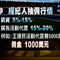
經紀人抽佣行情

美國36州州長改選

美國參院改選33席

美國眾院改選435席

美國對伊戰爭民調

民主黨奪眾院主導

高人鮑喜順236cm
分享:


常見的半導體材料有矽、鍺、砷化鎵等
/
晶片測試
晶片處理高度有序化的本質增加了對不同處理步驟之間度量方法的需求。晶片測試度量裝置被用於檢驗晶片仍然完好且沒有被前面的處理步驟損壞。如果If the number of dies—the 積體電路s that will eventually become chips—當一塊晶片測量失敗次數超過一個預先設定的閾值時,晶片將被廢棄而非繼續後續的處理製程。
/
晶片測試
晶片處理高度有序化的本質增加了對不同處理步驟之間度量方法的需求。晶片測試度量裝置被用於檢驗晶片仍然完好且沒有被前面的處理步驟損壞。如果If the number of dies—the 積體電路s that will eventually become chips—當一塊晶片測量失敗次數超過一個預先設定的閾值時,晶片將被廢棄而非繼續後續的處理製程。
/
步驟列表
晶片處理
濕洗
平版照相術
光刻Litho
離子移植IMP
蝕刻(干法蝕刻、濕法蝕刻、電漿蝕刻)
熱處理
快速熱退火Annel
熔爐退火
熱氧化
化學氣相沉積 (CVD)
物理氣相沉積 (PVD)
分子束磊晶 (MBE)
電化學沉積 (ECD),見電鍍
化學機械平坦化 (CMP)
IC Assembly and Testing 封裝測試
Wafer Testing 晶片測試
Visual Inspection外觀檢測
Wafer Probing電性測試
FrontEnd 封裝前段
Wafer BackGrinding 晶背研磨
Wafer Mount晶圓附膜
Wafer Sawing晶圓切割
Die attachment上片覆晶
Wire bonding焊線
BackEnd 封裝後段
Molding模壓
Post Mold Cure後固化
De-Junk 去節
Plating 電鍍
Marking 列印
Trimform 成形
Lead Scan 檢腳
Final Test 終測
Electrical Test電性測試
Visual Inspection光學測試
Baking 烘烤
/
有害材料標誌
許多有毒材料在製造過程中被使用。這些包括:
有毒元素摻雜物比如砷、硼、銻和磷
有毒化合物比如砷化三氫、磷化氫和矽烷
易反應液體、例如過氧化氫、發煙硝酸、硫酸以及氫氟酸
工人直接暴露在這些有毒物質下是致命的。通常IC製造業高度自動化能幫助降低暴露於這一類物品的風險。
/
Device yield
Device yield or die yield is the number of working chips or dies on a wafer, given in percentage since the number of chips on a wafer (Die per wafer, DPW) can vary depending on the chips' size and the wafer's diameter. Yield degradation is a reduction in yield, which historically was mainly caused by dust particles, however since the 1990s, yield degradation is mainly caused by process variation, the process itself and by the tools used in chip manufacturing, although dust still remains a problem in many older fabs. Dust particles have an increasing effect on yield as feature sizes are shrunk with newer processes. Automation and the use of mini environments inside of production equipment, FOUPs and SMIFs have enabled a reduction in defects caused by dust particles. Device yield must be kept high to reduce the selling price of the working chips since working chips have to pay for those chips that failed, and to reduce the cost of wafer processing. Yield can also be affected by the design and operation of the fab.
Tight control over contaminants and the production process are necessary to increase yield. Contaminants may be chemical contaminants or be dust particles. "Killer defects" are those caused by dust particles that cause complete failure of the device (such as a transistor). There are also harmless defects. A particle needs to be 1/5 the size of a feature to cause a killer defect. So if a feature is 100 nm across, a particle only needs to be 20 nm across to cause a killer defect. Electrostatic electricity can also affect yield adversely. Chemical contaminants or impurities include heavy metals such as Iron, Copper, Nickel, Zinc, Chromium, Gold, Mercury and Silver, alkali metals such as Sodium, Potassium and Lithium, and elements such as Aluminum, Magnesium, Calcium, Chlorine, Sulfur, Carbon, and Fluorine. It is important for those elements to not remain in contact with the silicon, as they could reduce yield. Chemical mixtures may be used to remove those elements from the silicon; different mixtures are effective against different elements.
Several models are used to estimate yield. Those are Murphy's model, Poisson's model, the binomial model, Moore's model and Seeds' model. There is no universal model; a model has to be chosen based on actual yield distribution (the location of defective chips) For example, Murphy's model assumes that yield loss occurs more at the edges of the wafer (non-working chips are concentrated on the edges of the wafer), Poisson's model assumes that defective dies are spread relatively evenly across the wafer, and Seeds's model assumes that defective dies are clustered together.[25]
Smaller dies cost less to produce (since more fit on a wafer, and wafers are processed and priced as a whole), and can help achieve higher yields since smaller dies have a lower chance of having a defect. However, smaller dies require smaller features to achieve the same functions of larger dies or surpass them, and smaller features require reduced process variation and increased purity (reduced contamination) to maintain high yields. Metrology tools are used to inspect the wafers during the production process and predict yield, so wafers predicted to have too many defects may be scrapped to save on processing costs.[26]
我爽就好
自發對稱破缺是一種既保持原有拉格朗日量對稱性,又能使得最終描述的系統破壞此對稱性的機制。[1]:347
我看A片上慈惠醫院曾文蘭女優的陰道